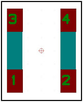
It is an inductor where the datasheet asks for 2 long pads but with only the ends of the pads being exposed for soldering to.
The question was - How to do this ?
If you look at the footprint information supplied:
You can see from this footprint that the shaded area (which is solder resist) effectively separates the 2 long pads into 4 smaller exposed pads where each pair are joined together under the resist.
This can easily be achieved in CADSTAR by adding 4 pads and connecting them together using component copper, I shall show you how.
First figure out from the drawing how big the 4 pads need to be and add 4 rectangular pads so that the left 2 are pads 1 and 3, the right 2 are pads 2 and 4 as follows.
(The reason for this is that the inductor symbol has only 2 terminals so you can identify them as pads 1 and 2.)
Then add some component copper that covers pads from pad 3 down to pad 1 and from pad 4 down to pad 2 as follows.
That will provide you with the required 2 large copper pads but with 4 exposed areas, however as far as your netlist goes pads 1 and 2 are connected to your circuit, pads 3 and 4 are not and you will get component copper to pad errors.
To prevent these errors and connect pads 1 and 3 together with the copper, in the copper properties enter the pad numbers (identifiers) for both pads.
What this will do is electrically connect them together, so in the part you only need to allocate pin 1 and 2, then when connecting to pin 1 - pin 3 is connected via the copper (Max pins = 2).
You can only connect 2 pads together like this so if you are wanting to connect more than 2 together you simply use more pieces of component copper and daisy chain them together etc.
So you will end up (once you have added the outlines etc) with a component footprint that looks like:
For similar components - perhaps where the datasheet calls for a pad shape not supported by CADSTAR, you can create the shape with component copper and attach it to a pad that covers as much of it as you can, 99 out of 100 time this is more than adequate for the component.
Any problems - post a comment.
Addendum.....
When creating the symbol it must have only 2 terminals, using 4 will enable you to add 4 nets to it in the schematic and in the PCB it will need to be only 2 - 4 will produce an error.


5 comments:
Is this apply to SOT223 packages too ? E.g.: linear regulators such as LT1117 ?
With Pulsonix it is possible to assign a logic pin to more than one physical pins. I was not able to find this functionality in CADSTAR :(
thanks
No, this only applies when a copper connection is required between the 2 pads.
In that case, the component copper can join 2 pads together to the same net.
If you want SOT233 pins 2 and 4 to both be on the same signal then simply add both pins to the symbol and connect them both in the schematic.
Thanks for the answer. It is sad anyway. In this case I have to add a new pin in the symbol.... thanks anyway
You do not need to add any more pins in the schematic symbol - read what I said above.
In a word - no.
You are suggesting explicit pin/net names but want to change them.
If you define the signal name on a pin in the part, this pin name is not visible or changeable in the design, in fact if you do not have that signal available then the pin is not connected. This is the way it used to be for the older 74 series IC's etc however modern devices need more pins on different nets and its far better for them to be available in the design.
Add the power pins to a power block which you can put on another sheet so they are still available yet do not need to be part of the main schematic. Although not having the pins visible to the reader makes it problematic as they wont know what pin does what.
This is why explicit pins is a legacy feature that is little used now and I would certainly not be using it in a FPGA chipped design.
Post a Comment